Circuit
The circuit has been developed using an ATmega88PA. This time completely in THT so it can be built up with simple means on a breadboard.
During the development process it has been put to its limits. Not a single pin is left unused. (Indeed, the pins of the programming interface could still be used with limitations.)
If you cut down some of the gimmicks it might even fit into an ATmega48, having only 4 k Flash. My actual version does not...
In the sources you can also select an ATmega8a via #define which I accidentally ordered at first. It is pin compatible but we use a different timer then. The only loss is the missing temperature sensor but we don't use it until know, anyway.
The compiled version has to fit the selected controller. They are not binary compatible!
Indeed, the only controller I used up to now is the AT
Seven-Segment Display
I chose a newer type achieving good brightness even with relatively low currents. The ATmega drives the segments directly from a port pin from its VCC against GND. For the common cathodes I used a relay driver ULN2803 since the current here is too much for a simple port pin. It is significantly smaller and with 30 cents probably even cheaper than a discrete circuit consisting of six (Darlington) transistors plus base resistors plus the additional PCB area. Of course I could even have selected the ULN2003 which has only seven drivers (we need only 6) being even a little bit smaller and may be even cheaper but I had the 2803 in stock...
Indeed you can also use the ULN2003, it has to be fitted right-aligned
i.e.
pins 1 and 18 remain open.
We also have to pay special attention to the segment drivers (i.e. the corresponding port pins since there are no additional drivers in between). The allowable current of 20 mA is well ok but the datasheet specifies a maximum of 100 mA per port so we must not connect all segments to one single port! This complicates the software a little bit but it isn't a real mess.
The gain with this is that we can keep clear the programming interface from additional loads.
Especially when using cheap programmers from the Ebay selection you can not be sure if they can keep the levels and rise times necessary for a reliable programming when loaded with 20 mA.
Attention: the segment driver pins are not configured as output!
The pin is permanently 1
and the DDR
controls which segments are on!
Here you can see why.
Main Switch
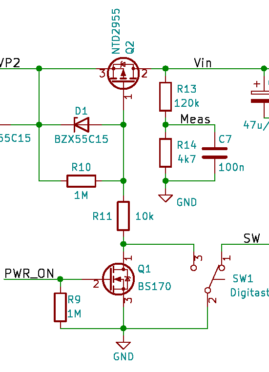
The scale is powered on by pressing button SW1 which controls the MOSFET Q2 directly. When the controller is started, it controlls the power via Q1, which shorts the make contact of the button. So the controller can also turn off when there is no activity for some time. This circuit has nearly no standby loss and is equivalent to a latching button we had to add otherwise.
To keep the button operational after power on, we use its break contact (line SW
).
The button we use is a high-grade button (Shadow Digitast), you'll experience a sophisticated tactical feeling
and high endurance. Cheaper buttons would work the same, but not as long and not as professional.
Note: R13/R14 and C7 are only for monitoring the voltage and are not needed for switch operation.
If the button had no break contact, we could manage this by adding two diodes and a transistor. I leave it to you as a brainteaser where they should be 😜.
For the unsportsmanlikes and the curious, here
is a simulation1 for LTspice.
Practice showed that you have to press the button unexpectedly long to switch on the scale. There is a small delay in the firmware (50 ms) to prevent the scale from switching on again just after the controller powered off but it showed that it takes additional 450 ms to go there. This seems to be the startup time of the RC oscillator which is not specified in the datasheet. The ATMega8a needs nearly half a second after power on (with RC oscillator) before executing its first instruction...
Reverse Polarity Protection
The power supply as well as the battery may be connected in reverse polarity. To prevent damage, we could put a diode in series. But it would due to its voltage drop increase the power loss and thus reduce battery life. (at 9 V for about 8%, so no problem for a china device)
Else we could put a diode in parallel, shortening reverse voltage. If we had a powerful supply, the diode would fail
and we even had to fuse it to prevent more damage.
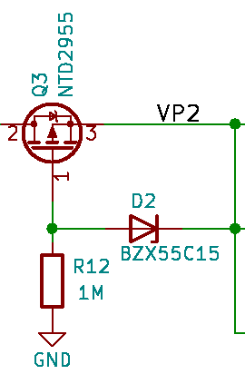
That's why I invested 40 cents here to realize reverse polarity protection with a P-
 It is on only when the polarity is correct and is off when not.
D2 limits the gate voltage and so this circuit is safe up to the breakdown voltage of the MOSFET (60 V),
far more than the maximum operating voltage of the scale.
Indeed the 2×40 cent (reverse polarity protection and main switch) are pure overkill since the MOSFET allows much more current (12 A!) than we need but we just had it in stock... At least, it does not require a heatsink! Maybe you can do that with 20 cents if it is necessary. A tiny BSS84 (-130 mA ID) can not do it (except for a china device 😉).
Besides this, the BSS84 with a typical on resistance of 6 Ω even at only 65 mA
would cause a voltage drop of 0,4 V (nearly as much as a cheep diode) and contribute to
higher loss and lower battery life.
The NTD
The MOSFET hardly induces any voltage drop (at 200 mA roughly 36 mV resulting in about 7 mW) and draws nearly no current in reverse direction and thus is safe up to its breakdown voltage of 60 V and so it is even safer than the voltage regulator itself, allowing only 40 V. You can of course break anything if you want to... With this values it is far in advantage compared with a simple diode, saving roughly 8% of battery with only moderate additional costs.
Just to tell that in real life, assuming a battery life of one year, this circuit gives an additional month!
Financially, this may be not a real profit (at least not now) but ecologically it probably is!
The zener diodes D1 and D2 limit the gate voltages to an acceptable value. If you are sure that no more than 20 V may be connected, you may also omit them. But they are not really expensive. Maybe someone in spite takes a 24 V wall wart which is on its upper limit of 26 V and may be strong enough to shoot through the gate... Better safe than sorry!
You could now get the idea to use the transistor for reverse polarity protection as main switch at the same time but unfortunately this trick doesn't work because even with Q3 switched off, current would still be conducted via its body diode 😠.
Would you have thought of that? Therefore it is useful to simulate even such simple
circuits under all circumstances before building them!
Debug Interface
Unfortunately, the pins of our preferred debug interface, RS232, are already occupied. Only the SPI interface is available, even very comfortable on a 6-pin header! This is sufficient for debug messages. Just send the data via SPI and decode it with your logic analyzer (maybe a Saleae Logic 8 which is not only a good looking instrument but is really worth every dollar you paid for it). It will show the bytes in hex, dec or ASCII, just like you want.
I must admit that debug input is problematic but was not really necessary up to now.
1 This is just a simulation I never built up in real life. In my expierience, simulation hits reality in a quite accurate way.


