Luxmeter Experiment
I granted myself an experimental project working with photo diodes. I must emphasize that I never had to work with photo diodes (but I've seen one, though). A simple PCB has been developed to test two versions:
- A luxmeter-
version using a photo diode in the spectral range close to human eyes - A fast version dedicated to detecting short and fast rising pulses
Both versions can be build on the same PCB. The circuit is supplied by 5 V DC and generates
the -5 V for the symmetric supply of the OpAmp internally.
It has a low-
Have a look at the circuit and the
Target
General Considerations
Photodiodes can be operated in reverse direction or in photovoltaic mode. In reverse direction they have a leakage current proportional to lighting over several decades. In photovoltaic mode they generate a photo current which is also proportional to the lighting. In each mode, we are talking about a few nA per Lux. Current in the range of nA (0.000,000,001 A or merely ~6,000 electrons per µs) is pretty low and is subject to get lost somewhere!
The measurement will primarly target to eliminate the leakage or photo current and thus keep a constant voltage over the diode. So you can avoid to charge the juction capacitance of the diode which can be relatively high. The BPW21 for example has a junction capacitance of more than half of a nanofarad. Charging it with a few nA would seriously degrade the bandwith of the circuit!
If we do not want to limit the circuit to high intensities, the opamp amplifying the signal must meet some requirements:
- If we have only nA as a signal, it must have a low offset/bias current. A µA741 or even a relatively new TLC272 will not fit.
- If 0 nA should translate to 0 V, the offset voltage has to be minimal. 10 nA produce only 10 µV over the 1 kΩ feedback resistor! If the opamp has only 1 mV offset we are 100 Lux off (at the low gain output)! The TLC272 with 10 mV offset voltage is completely inappropriate.
The layout is also a challanging task. 100 MΩ of insulation resistance
at 5 V cause a leakage current of 50 nA! Guard rings are needed to avoid high
differential voltages with respect to the sensitive signals.
The manufacturing has to be clean
since dirt of all kinds (especially skin sweat, remains
of the liver sausage from the morning break etc.) may have serious impact on the
insulation resistance of the board!
Of course you can wash the boards afterwards but it is better not to contaminate
them at all.
The circuit requires a symmetrical supply. From the +5 V supply voltage, -5 V are generated on board and are low noise filtered so a single +5 V supply is sufficient. You must not connect a negative supply at the -5 V pin! On this pin, the internally generated -5 V are available for measuring purposes or to supply a few mA to the following circuit!
Option 1 uses a BPW21 which is optimized for visible light (in the datasheet the sensivity is specified in nA/Lux, accordingly) and a relatively slow and cheap opamp type LTC2051). It has a very low offset value of 3 µV as well as a low bias current of 50 pA (at room temperature). The costs are at 4€ what is, well, affordable.
The diode operates in photovoltaic mode here and the opamp compensates the photo current keeping the voltage over the diode at 0 V.
Option 2 uses a BPW24 which is significantly faster. Its sensivity is mostly in near infrared
and is therefore specified in A/W (photo current per radiant power).
It is biased with -5 V to lower the junction capacitance and thus rise its
speed. A higher voltage would make it even faster but the following circuit would have to match
this (and you have to generate the voltage somehow).
Fitting this demands, a much faster opamp type LT1469 was selected.
It will raise the costs of the cirquit significantly!
Until now, I could not verify how fast the circuit really is since I do not have a light source
with the required short (and defined) rise time.
A circuit like this would probably be used for fast data transmission.
A simple trim potentiometer is used to calibrate the sensivity. If you happen not to have a reference light source, just measure the value of the pot (without supply, of course) and set it to 1 kΩ. For option 1, the low gain output has about 10 µV per lux and the high gain output about 1 mV per lux. 1 mV may seem very low but illuminated with one lux you could hardly see anything! In your office there is a minimum illumination of 500 Lux and then we have already 0.5 V. When the sun is shining it will be some more and if you turn the diode towards a bright surface or even towards the sun, the high gain output will soon meet its limit!
The low gain output is made to show short, bright flashes like those used in photography.
Experiment: measuring a Photo Flash
Have a look at some oscillograph curves of a Canon 420EX flashlight, recorded with the low speed option (with the BPW21).
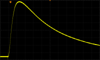
- An uncontrolled flash (caused by the test flash button on the 420EX). All energy stored in the flash capacitor is converted to light. As you can see, the maximum brightness is reached after about 250 µs and flattens following an exponential curve. The brightness in my situation reaches about 150.000 Lux, a little bit more than what we could expect at a bright summer day.
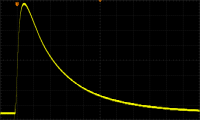
- The same thing in lower time resolution.
You can see that most of the energy is flashed in about 1.5 ms
(the total amount of light is about the area under the curve).
So a flashlight photograph is like a photograph at 1/1000 or 1/500 of a second.
Despite this, on the camera you have to select a relatively long exposure time of 1/125 or 1/60 seconds. The reason for this is that the shutter has to be completely opened before the flash fires (and has to stay opened until the flash has burned out). So even subjects in fast motion can be depicted relatively sharp. Although you may get a more balanced lighting using a longer exposure time (sometimes up to several seconds) using available ambient light. The flash is then used as a fill flash to light up the nearby (but shadowed) subject while it has due to the distance no effect on the far beach, which is lighted by the noon sun. A good camera will choose a well balanced flash energy depending on the exposure time you selected.
Photos which did not follow this rule can be found numerously in the internet and show a perfectly lighted (or slightly too bright) subject in front of a mostly black background... - Here comes a real photography, in time lapse. You can see the measure flash and about 75 ms later, the main flash (the trigger (the orange colored T) is on the main flash).
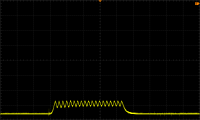
- This is the measure flash. Indeed, it looks like a switched constant current source, just like a LED lamp. The flash produces a constant light for a defined time and the flash unit can calculate the amount of light necessary for a perfect lighting.
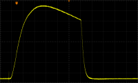
- And here the main flash.
The initial curve form is identical to the uncontrolled flash but it is terminated
as soon as the needed light is reached.
In early flash devices this was achieved by a SCR shorting the flash bulb and eliminating the remaining energy (what could be heared as a distinctiveplop
). Nowadays, the current is interrupted by sophisticated circuits, a MOSFET or an IGBT. So the remaining energy can be reused for the next flash. This not only saves battery but also increases the flash rate.
I find it fascinating how deep you can zoom into the oscillogram on modern oscilloscopes. In fact, the pictures of the measurement and main flash are just magnifications of the picture time lapse which has been recorded at 25 megasamples per second (at a record length of six megasamples!).
It is also clear that the measurement flash must not be used to expose the picture as it would look like a double exposure. Exposure begins just with the main flash. The energy of the measure flash will be lost for the exposure. This is mandatory as even the measure flash might be too bright for a good exposure. The 75 ms also include the time necessary to completely open the shutter of the camera.


